Online Basic Digital Electronics Course with Lab
1. Introduction
What you will build
Digital circuits that are found inside microcontrollers.
What you will learn
Design the following 4 combinational logic circuits and breadboard them in your home laboratory.
- 1 to 2 Demultiplexer
- Half Adder
- 4 to 2 Priority Encoder
- 2 bit Comparator
What you will need
- Raspberry Pico with pre-soldered headers
- USB cable
- Breadboard
- Jumper wires
- the following 74HC series low voltage logic ICs in DIP
- 74HC04 NOT Gate x 1
- 74HC08 AND Gate x 2
- 74HC32 OR Gate x 1
- A recent version of Chrome (89 or later) on a computer (Windows, MacOS, Linux or ChromeOS)
2. About Combinational Logic Design
Combinational Logic uses a combination of basic logic gates AND, OR and NOT to create complex functions. For each output, the design procedure is:
- Derive the truth table.
- Simplify the boolean expression using Karnaugh Map (K map).
- Draw a logic diagram that represents the simplified Boolean expression. Verify by analysing or simulating the circuit.
Required reading
3. 1 to 2 Demultiplexer
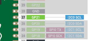
In the Raspberry Pico, Pin 27 can be used either as a DIO1 (GP21) or a I2C Clock (I2C0 SCL). In the Pico, a Select input to a 1 to 2 Demultiplexer routes Pin 27 to either the DIO or the I2C Clock.
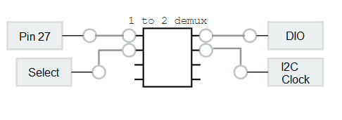
In your first exercise
- Learn how to design a 1 to 2 Demultiplexer. Since there are 2 outputs, you will need to design 2 times - first for DIO and a second time for the I2C Clock.
- Practise to breadboard the circuit correctly on the simulator
- Do it on a real breadboard and observe the results
Note 1: GP 21 of the Pico is a Digital Input/Output. Our design only works for the digital input part.
4. Half Adder
In microcontrollers, a counter is commonly used in programming. A typical instruction is i = i + 1 where 1 is added to the variable i. In this exercise you will learn how addition is implemented in digital electronics.
In elementary arithmetic, a carry is a digit that is transferred from one column of digits to another column of more significant digits. The concept of carry is the same regardless we are doing decimal or binary maths.
The half adder is a digital circuit that adds two one-bit binary numbers A and B. The output is the (S)um of the two bits and the (C)arry.
- 0+0 -> C = 0, S = 0
- 0+1 -> C = 0, S = 1
- 1+0 -> C = 0, S = 1
- 1+1 -> C = 1, S = 0
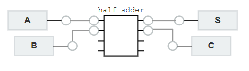
In this exercise
- Learn how to design a Half Adder. Since there are 2 outputs, you will need to design 2 times - first for (S)um and a second time for the (C)arry.
- Practise to breadboard the circuit correctly on the simulator
- Do it on a real breadboard and observe the results
Understanding of basic binary arithmetic is required for this exercise. See binary addition if you need further information.
5. 4 to 2 Priority Encoder
Interrupts are used in microcontrollers to allow it to respond to external events by suspending current processing and switching to the routine to service the interrupt. Below is the top 4 in priority order of the interrupts of the Atmega328 microcontroller used in the Arduino.
- Reset
- External Interrupt Request 0 (pin D2)
- External Interrupt Request 1 (pin D3)
- Pin Change Interrupt Request 0 (pins D8 to D13)
The priority order means that regardless what happens to 3, 4 if 2 External Interrupt Request 0 occurs, it will be executed and the rest of the interrupts will have to wait until 2 is serviced. If there are ONLY 4 interrupts, a 4 to 2 Priority Encoder can be used to implement this function.
A 4 to 2 priority encoder provide 2 bits of binary coded output representing the position of the highest order active input of 4 inputs. If two or more inputs are high at the same time, the input having the highest priority will take precedence. In this design I3 has the highest priority and I0 the lowest .
In this partial truth table, for all the non-explicitly defined input combinations (i.e. inputs containing 2, 3, or 4 high bits) the lower priority bits are shown as don't cares (X). Similarly when the inputs are 0000, the outputs are not valid and therefore they are XX.
| I3 | I2 | I1 | I0 | O1 | O0 |
| 0 | 0 | 0 | 0 | X | X |
| 0 | 0 | 0 | 1 | 0 | 0 |
| 0 | 0 | 1 | X | 0 | 1 |
| 0 | 1 | X | X | 1 | 0 |
| 1 | X | X | X | 1 | 1 |
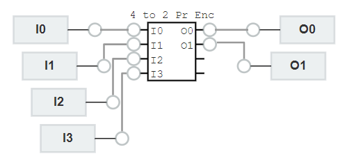
- Learn how to design a 4 to 2 Priority Encoder. Since there are 2 outputs O0 and O1, you will need to do 2 designs, one for each output
- Practise to breadboard the circuit correctly on the simulator
- Do it on a real breadboard and observe the results
6. Comparator
Design a circuit that compares two 2-bits natural numbers A (A1,A0) and B (B1,B0) providing an output S such that
- S = 1, if A > B
- S = 0, otherwise
Note: A1, B1 is MSB (most significant bit) and A0, B0 is LSB (least significant bit)
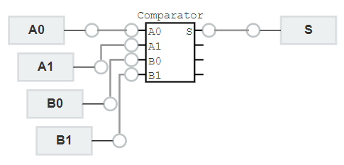
- Learn how to design a comparator.
- Practise to breadboard the circuit correctly on the simulator
- Do it on a real breadboard and observe the results
Understanding of basic binary arithmetic is required for this exercise. See binary addition if you need further information.
7. Congratulations
Congratulations! If you have completed all the 4 exercises successfully, you would have earned the following 2 digital badges.
Most importantly, you have acquired the basic skills to use simulation, analysis and measurement to learn further topics in digital electronics on your own or with your peers who have completed this course.