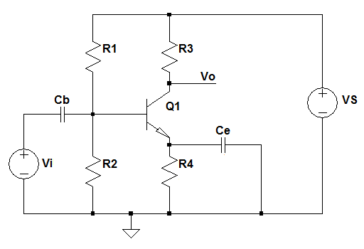
BJT Common Emitter Amplifier with emitter degeneration
A basic BJT common emitter amplifier has a very high gain that may vary widely from one transistor to the next. The gain is a strong function of both temperature and bias current, and so the actual gain is somewhat unpredictable. One common way of alleviating these issues is with the use of emitter degeneration. Emitter degeneration refers to the addition of a small resistor (R4) between the emitter and the common signal source.
In this circuit the base terminal of the transistor is the input, the collector is the output, and the emitter is common to both. It is a voltage amplifier with an inverted output. The common emitter bjt amplifier is one of three basic single-stage bipolar-junction-transistor (BJT) amplifier configurations.
DC Analysis
First we redraw the schematic using the BJT DC model. Capacitors are considered open circuit in DC and therefore are excluded.
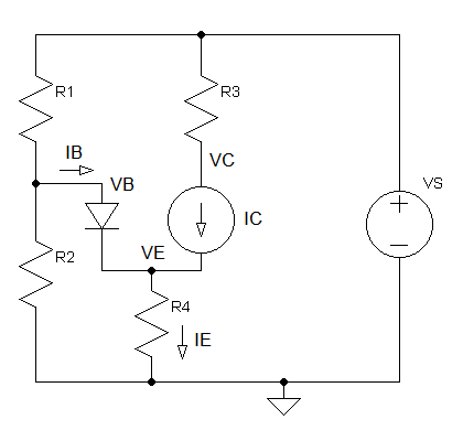
IB can be ignored if \begin{equation} 10R_2 < \beta R_4 \end{equation} Thus VB can be calculated using KVL as simple voltage divider circuit \begin{equation} V_B = {R_2 \over {R_1 + R_2}} V_S \end{equation} Current at Node E \begin{equation} I_E = I_B + I_C \end{equation} if IC is much greater than IB, IB can be ignored \begin{equation} I_E = I_C \end{equation}
Using KVL (Kirchhoff's voltage law) \begin{equation} V_B = I_ER_4 + V_{BE} \end{equation} \begin{equation} V_S = I_CR_3 + V_{C} \end{equation}
If you are designing rather than analysing the DC circuit, you should choose the resistor values such that VC is half the supply voltage. This is to obtain maximum output voltage swing.
\begin{equation} V_{C} = {V_S \over 2} \end{equation}AC Analysis
Next we redraw the schematic using the BJT small signal model. Capacitors are considered shorts in AC (R4 is shorted out by Ce) and DC supplies are connected to GND (ground). Calculate re
\begin{equation} r_e = {v_T \over I_E} \end{equation}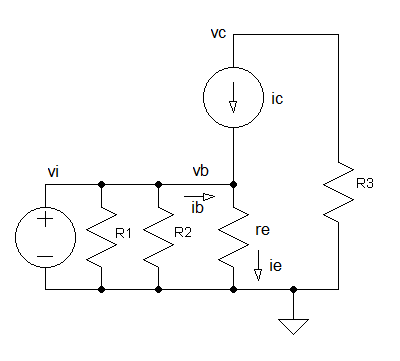
Since the input voltage vi is across re and using ohm's law
\begin{equation} i_e = {v_i \over r_e} \end{equation}The output voltage is \begin{equation} v_c = -i_cR_3 \end{equation} the inverted output is due to the current direction.
From KCL we know that \begin{equation} i_e = i_b + i_c \end{equation} By ignoring ib from the equation since it is small compared to ic, we obtain \begin{equation} v_c = -i_eR_3 \end{equation}
Applying equation 9 to equation 12, the voltage gain of the amplifier is \begin{equation} {v_c \over v_i} = -{R_3 \over r_e} \end{equation}