555 Timer
The 555 timer IC is an 8 pin integrated circuit used in a variety of timer, pulse generation, and oscillator applications. The 555 can be used to provide time delays or as an oscillator
The 2 common operating modes of the 555 timer IC are:
- Monostable mode: In this mode, the 555 functions as a "one-shot" pulse generator. Applications include timers, missing pulse detection, bouncefree switches, touch switches, frequency divider, capacitance measurement, pulse-width modulation (PWM) and so on.
- Astable (free-running) mode: The 555 can operate as an oscillator. Uses include LED and lamp flashers, pulse generation, logic clocks, tone generation, security alarms, pulse position modulation and so on.
The circuit below shows the 555 timer IC connected in the astable mode
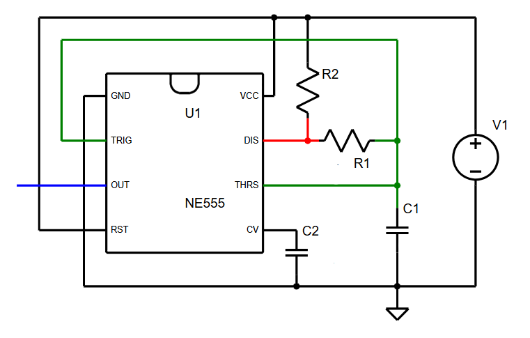
The output frequency is given by the following equation
\begin{equation} f_o = {1.44 \over (R_2 + 2R_1) C_1} \end{equation}The HIGH and LOW times of each pulse are given by
\begin{align} t_h &= 0.69(R_1 + R_2) C_1 \\ t_l &= 0.69 R_1 C_1 \end{align}Notes:
- Click on the colored nodes in the schematic to show/hide that node waveform.
- Select the different R1 and C1 values, press Simulate and observe the change in frequency and waveforms with the component values.
- Move the cursor in the chart to obtain the waveform values
Circuit Analysis
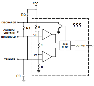
In order to analyse the 555 timings, we need to understand a little of the working of the 555 timer internally. There is a resistor tree with equal resistance values. They set the upper and lower limits of the capacitor charge/discharge voltage. Thus the voltages are
\begin{align} V_H &= {2 \over 3} V_{CC} = 0.66 V_{CC} \\ V_L &= {1 \over 3} V_{CC} = 0.33 V_{CC} \end{align}To derive the frequency equation of the 555 timer oscillator, we will make use of the universal time constant formula for the RC circuit.
\begin{equation} change = (f-s)( 1 - e ^ {-{t \over RC}}) \end{equation}- where
- change is the capacitor voltage change
- f is the capacitor voltage at infinity
- s is the initial voltage of the capacitor
For th (the period when output is high), the capacitor is charged from VL to VH through the resistors R1 + R2 from VCC. Thus
- Change = 0.33VCC
- Start = 0.33VCC
- Final = VCC
For tl (the period when output is low), the capacitor is discharged from VH to VL through the resistor R2 to 0V. DISCHARGE pin is switched to 0V by the transistor switch. Thus
- Change = -0.33VCC
- Start = 0.66VCC
- Final = 0V